
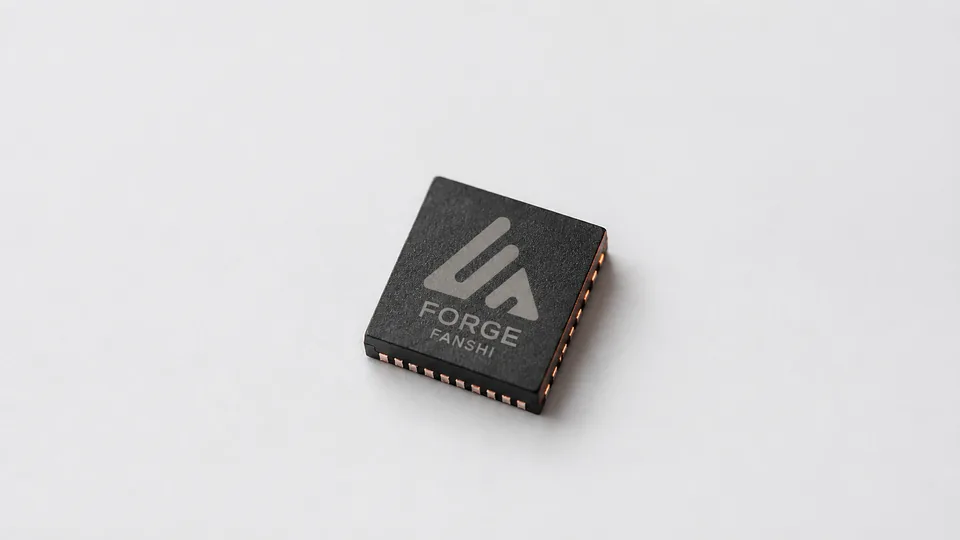
Forge
Lightweight edge chip
A complete language model inside a sub-watt handheld device.
17,000 token/s
The same inference cores and three routes can cast any model into silicon. Pick a chip that fits, or have one made for your model.
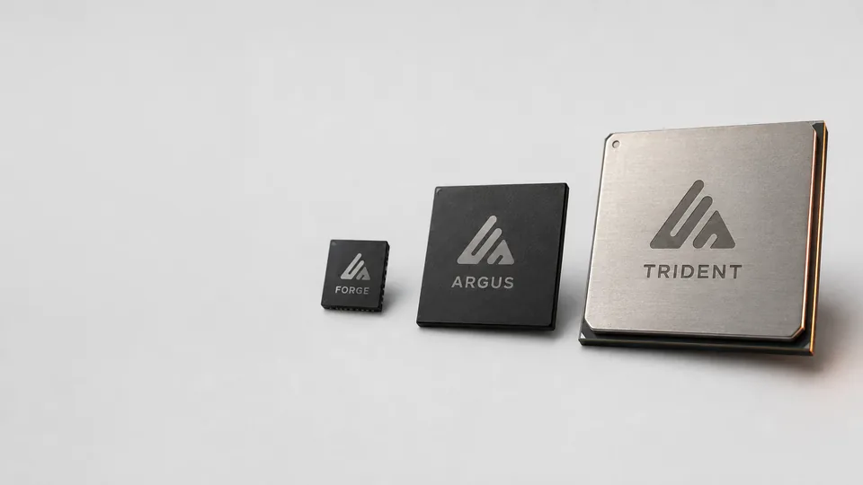
Lightweight edge chip
A complete language model inside a sub-watt handheld device.
17,000 token/s
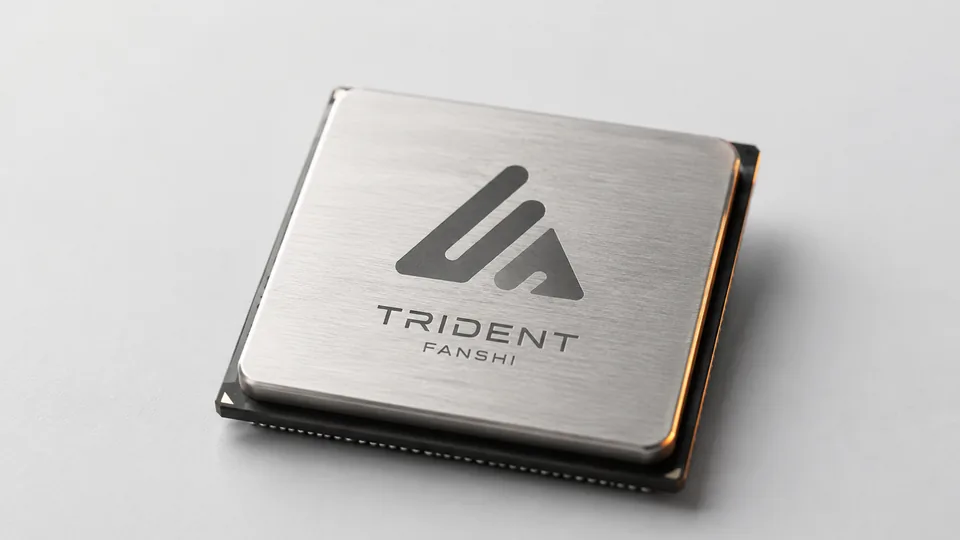
Flagship heavy-load chip
Run a 35B model locally at 15,000 token/s with a 70 W system budget.
15,000 token/s
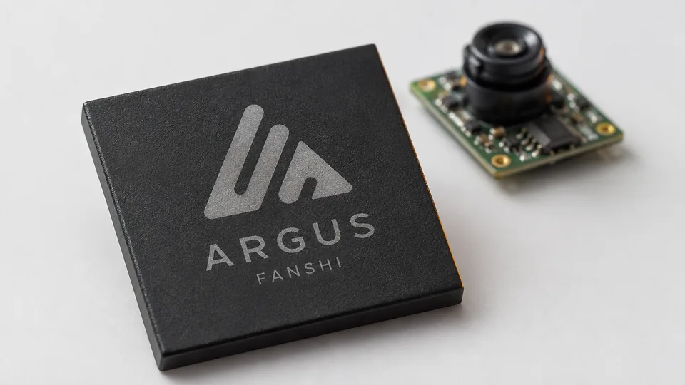
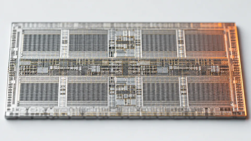
Made for your model
Your model, your chip. The same cores and routes, redefined around your model, power budget and volume.
0.6B → 35B+ model range
Figures on this page are current product definitions and design targets. Final specifications, test conditions, availability and delivery versions are confirmed per project.
01
Choose the route
Target model, performance and power goals, update cadence, interfaces. The first question is always: how often does the model change?
02
FPGA evaluation
Deploy the inference core on the evaluation board, run the model, measure accuracy and throughput: the first engineering sample.
03
System design-in
Interfaces, system software and field validation around the evaluation results, turning the sample into a product prototype.
04
ASIC delivery
Once the model is frozen: production ASIC, or the IP integrated into your own silicon.
Send the target model, performance goal, power budget and interfaces. We confirm the route and reply with a sample plan.