
Independent inference for every device.
Hefei Fanshi Semiconductor Technology Co., Ltd. builds edge LLM inference chips, inference IP and engineering validation platforms around compute-in-memory and near-memory compute, on a mature domestic 28 nm supply chain.
- Company
- 合肥燔石半导体科技有限公司
- Location
- Hefei, Anhui, China
- Process and supply chain
- Mature domestic SMIC 28 nm
- Routes
- MaskROM CIM · SRAM CIM · near-memory compute
- Products
- Forge · Trident · Argus
- Inference IP
- FS-Fusion · FS-Attention · FS-MoE · FS-Linear
- Contact
- info@fanshi-silicon.com
How we work with customers
01
Choose the route
Target model, performance and power goals, update cadence, interfaces. The first question is always: how often does the model change?
02
FPGA evaluation
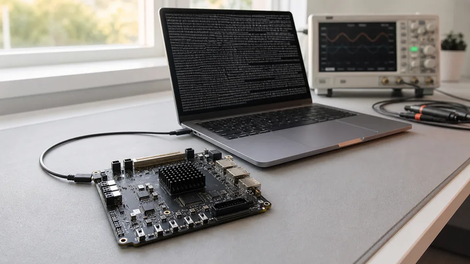
Deploy the inference core on the evaluation board, run the model, measure accuracy and throughput: the first engineering sample.
03
System design-in
Interfaces, system software and field validation around the evaluation results, turning the sample into a product prototype.
04
ASIC delivery
Once the model is frozen: production ASIC, or the IP integrated into your own silicon.
Products
Edge ASICs for lightweight language models, heavy-load inference and multimodal vision.
Technology
MaskROM, SRAM CIM and near-memory compute: three routes for different update cadences.
How we work
Engineering samples, FPGA evaluation boards, IP licensing and design-in support.
Contact Fanshi Semiconductor
Business, IP licensing, samples and hiring: info@fanshi-silicon.com.