
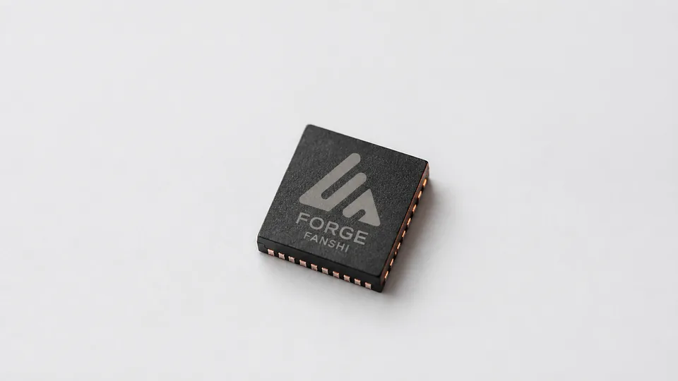
Forge
Lightweight edge chip
A complete language model inside a sub-watt handheld device.
17,000 token/s
Fanshi casts large models into compute-in-memory silicon: three routes, one inference core family, and a full path from model to tape-out. No network, no data leaving the device, near-zero marginal cost per inference.
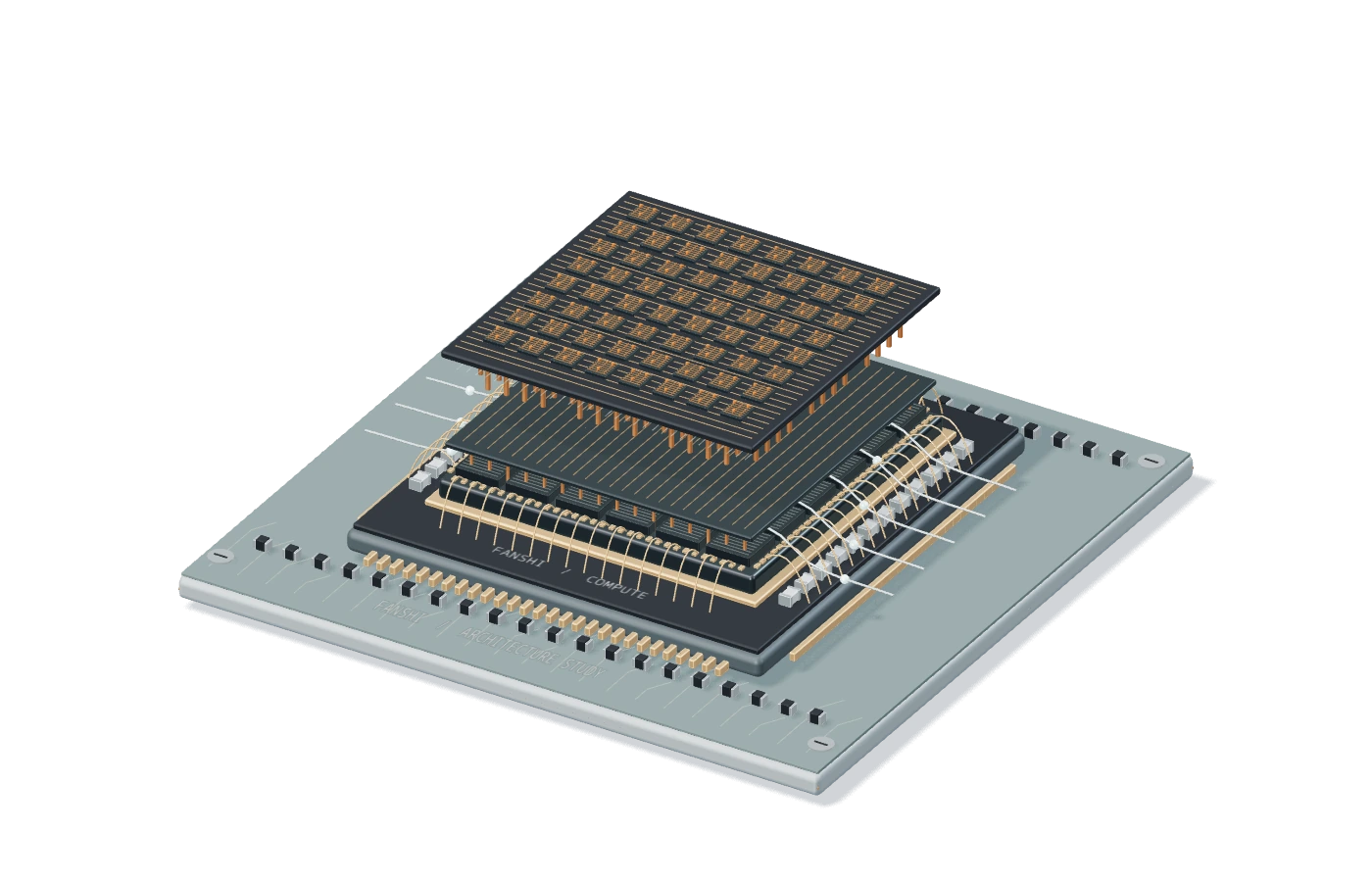
GPUs and NPUs spend most of their time and power shuttling weights between memory and compute. Fanshi turns that around: weights live in the memory array, and the math happens where they are.
让权重成为硅片的结构。
每 token 外部权重搬运
0MB
运行时保留
就地计算 · 无外部权重搬运
0.8B · INT8 估算,非整机功耗存算分离
传统 NPU / GPU 里,存储和计算是两块硅。生成每一个 token,全部权重都要经过总线走一遍:带宽就是上限,能耗大多花在路上。
存算一体
燔石把乘加电路做进存储阵列旁边:权重住在阵列里,激活流过去,结果流出来。总线上不再有权重。
MaskROM
掩膜存算一体在流片环节把权重物理写入通孔阵列。芯片出厂时模型已经在里面,功耗与单次推理的边际成本降到最低。
All three move weights less, or not at all. They differ in where the weights live and whether the model can still change. The first question to answer: how often does your model change?
On-device decode speed
Forge design target, Qwen 3.5 0.8B
System power
Forge lightweight edge class
Data stays on device
Local inference, no network required
Marginal cost per inference
After a one-time chip purchase
The same inference cores and three routes can cast any model into silicon. Pick a chip that fits, or have one made for your model.
Lightweight edge chip
A complete language model inside a sub-watt handheld device.
17,000 token/s
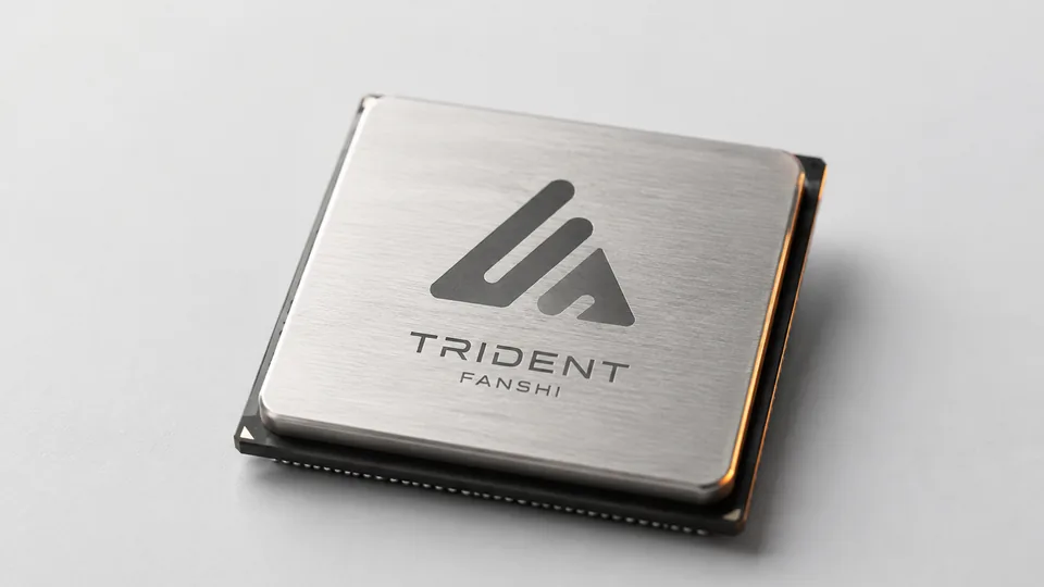
Flagship heavy-load chip
Run a 35B model locally at 15,000 token/s with a 70 W system budget.
15,000 token/s
Figures on this page are current product definitions and design targets. Final specifications, test conditions, availability and delivery versions are confirmed per project.
License Fanshi inference cores into your own ASIC or FPGA. One core family, four architectures, running on an evaluation board first.
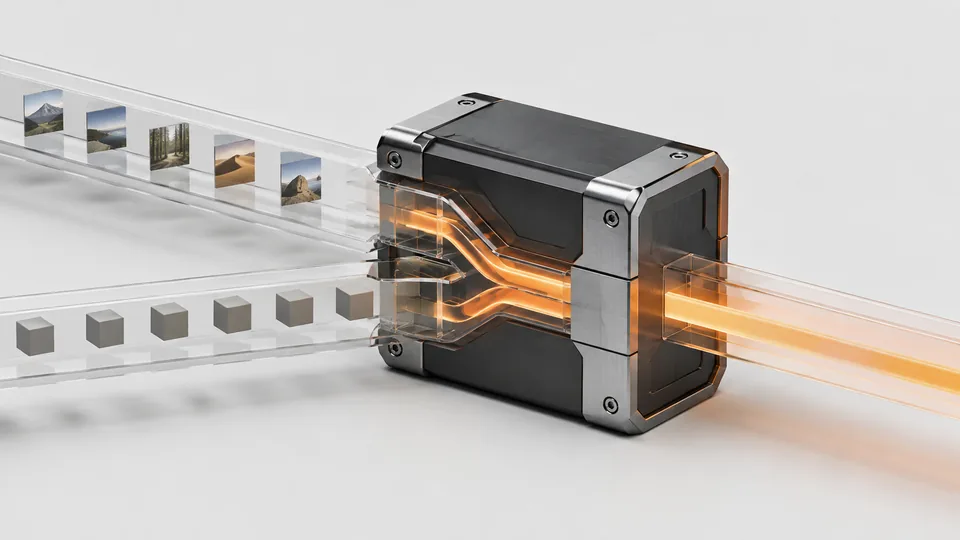
Joint vision-language understanding (VLM) and multi-sensor fusion, computed in place at the edge.
Native SmolVLM + SegFormer MiT fusion pipeline
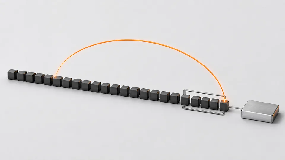
Native support for hybrid-attention large language models.
Qwen3 / 3.5 (0.6B to 9B) and SmolLM2
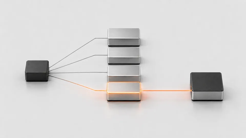
Built for dynamically activated sparse models, carrying large parameter counts within limited bandwidth.
Large sparse models on edge budgets
Linear attention and RNN-style architectures such as DeltaNet.
Very low latency streaming with unbounded context
That is how the production chips were made. Yours can follow: run it on an FPGA first, then decide between an existing chip and one of your own.
01
Choose the route
Target model, performance and power goals, update cadence, interfaces. The first question is always: how often does the model change?
02
FPGA evaluation
Deploy the inference core on the evaluation board, run the model, measure accuracy and throughput: the first engineering sample.
03
System design-in
Interfaces, system software and field validation around the evaluation results, turning the sample into a product prototype.
04
ASIC delivery
Once the model is frozen: production ASIC, or the IP integrated into your own silicon.
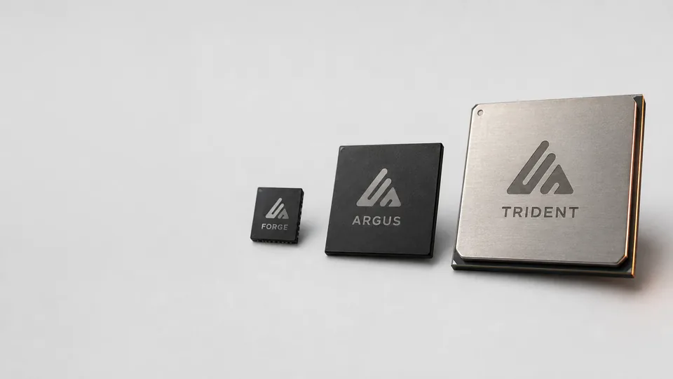
ASIC chips for edge LLM inference (Forge, Trident, Argus), FPGA evaluation boards, and inference core IP (FS-Fusion, FS-Attention, FS-MoE, FS-Linear) that can be deployed into a customer ASIC or FPGA.
Compute-in-memory performs multiply-accumulate inside the memory array, so weights never leave the storage cells. Near-memory compute places compute units next to high-bandwidth memory and uses on-chip streaming to minimise data movement. The first gives the lowest power and marginal cost; the second suits models that keep evolving.
Not on the MaskROM route: weights are fixed at tape-out. SRAM compute-in-memory loads weights at boot and can be updated. Near-memory compute keeps weights in external memory and supports continuous iteration.
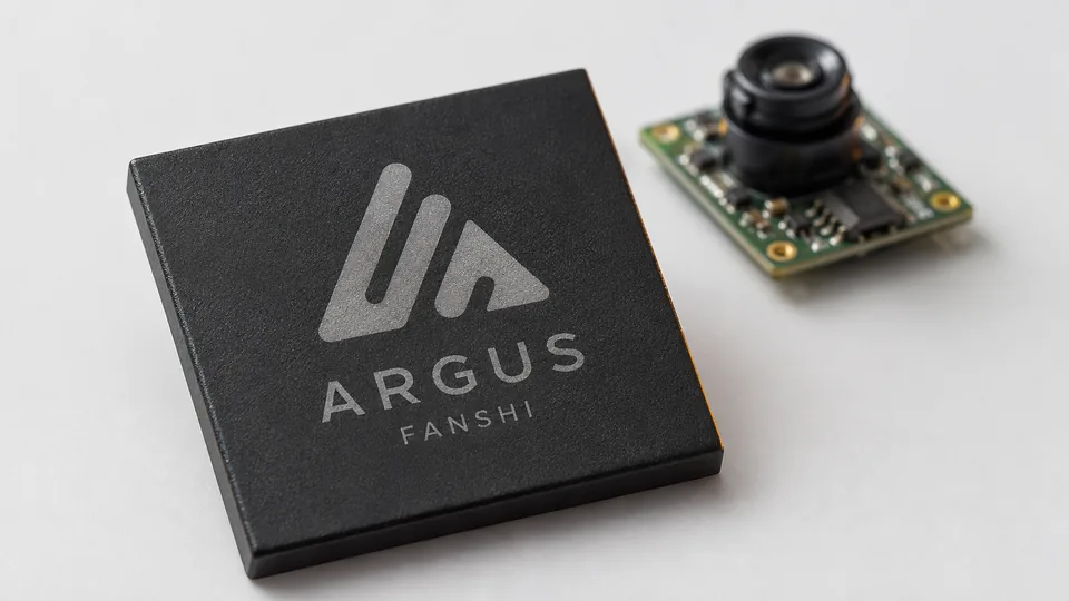
Forge targets Qwen 3.5 0.8B; Trident supports up to Qwen 3.5 35B; Argus runs SmolVLM, SegFormer and similar vision models. The IP family covers Qwen3 / 3.5 (0.6B to 9B), SmolLM2, sparse MoE models and DeltaNet-style linear attention.
They are decode-throughput design targets for the core model listed with each product. Exact model, precision, batch size and test platform are confirmed per project. The live demo on the site shows the measured decode rate of that conversation.
Send the target model, performance and power goals, interfaces and timeline. We reply with a route and an evaluation plan.